
A promising start for semiconductor research with X-rays and neutrons - theme kick-off
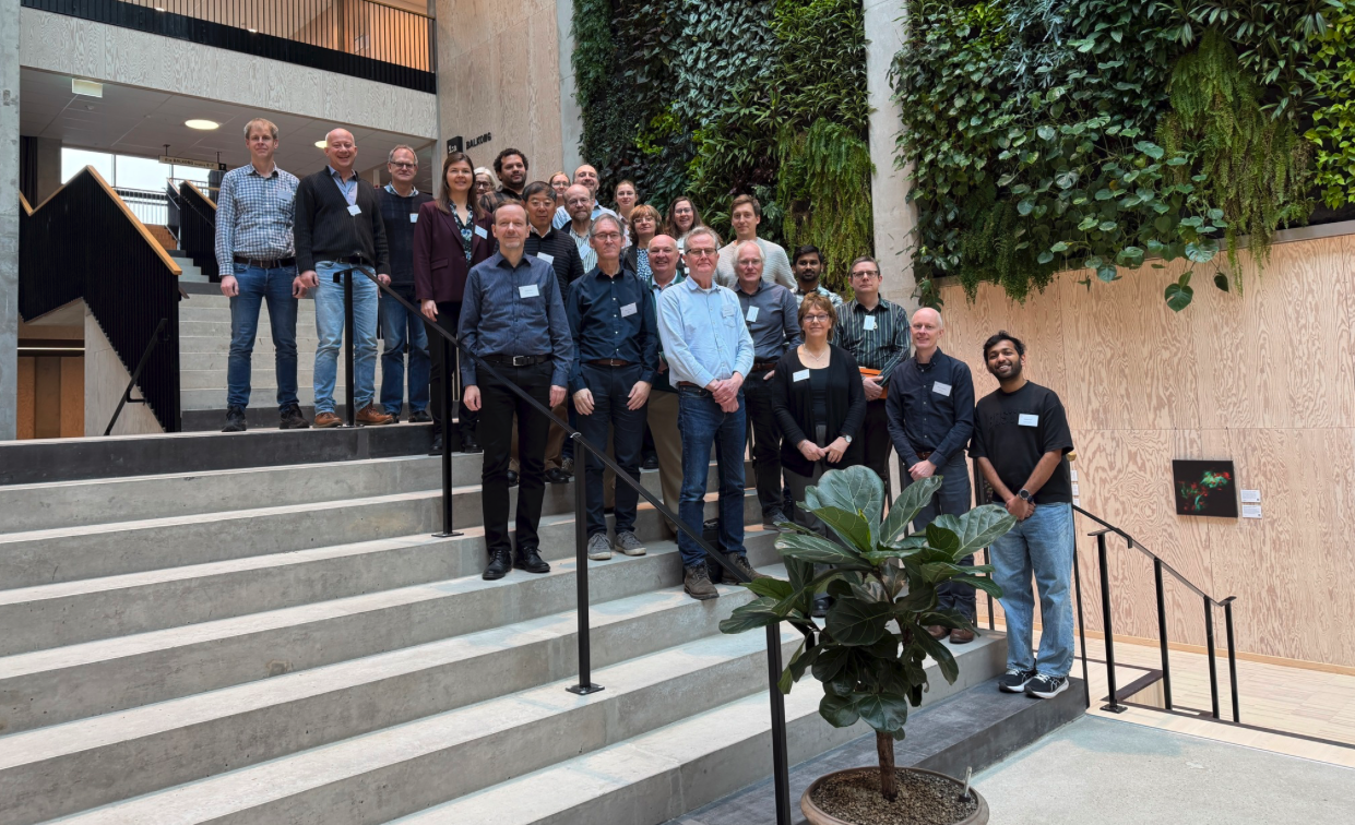
The participants at the Semiconductor theme kick-off pictured in The Loop.
The LINXS Semiconductors theme aims to combine semiconductor device development with advanced characterisation using X-rays and neutrons. In February, the theme had its first event at LINXS to plan its future work.
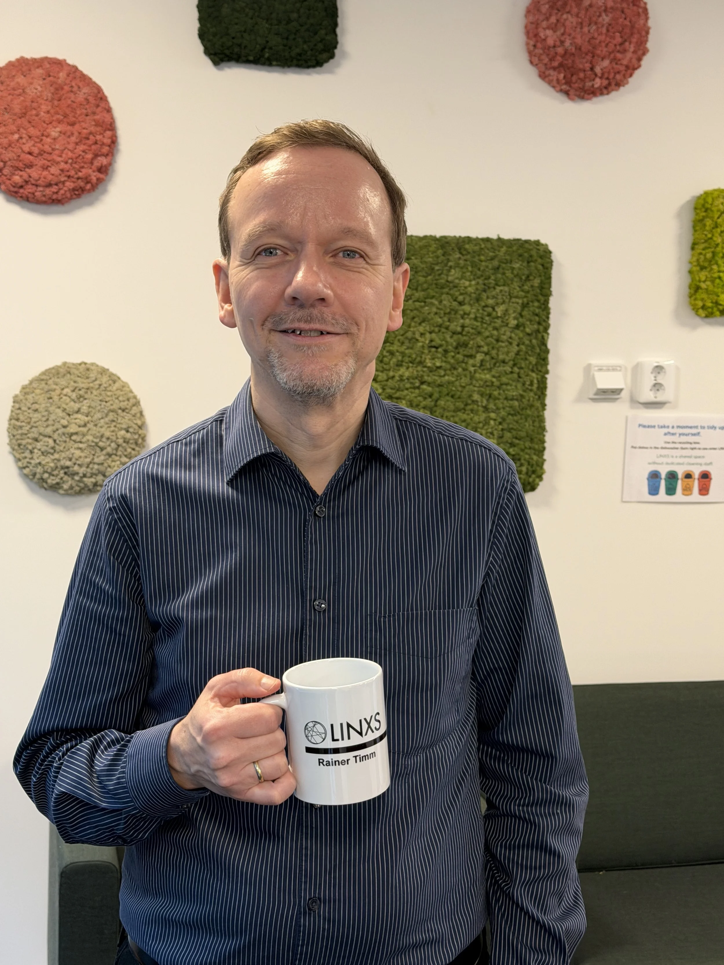
Rainer Timm is leading the LINXS Semiconductors theme.
“It was a very good experience,“ says theme leader Rainer Timm, Professor at the Department of Physics, Lund University. “We had many people in attendance and lively discussions right from the start.”
During the event, they had two parallel workshops to identify key needs and focus areas for the different working groups. The intention is to focus on the most pressing questions for developing semiconductor technologies.
“We want to improve what is well established within the field with new functionalities. We can never replace silicon, but we need to develop alternative technologies for more energy-efficient AI systems, and we need to ensure that novel semiconductor materials can support the green transition through improved electrification,” says Rainer Timm.
Bridging device development and beamline expertise
Many new materials are already being developed, emphasises Rainer Timm. Through advanced X-ray and neutron characterisation, their functionalities can be understood, refined and tested in ways that have not been possible before. Yet this will require experiments that produce data on how semiconductors operate in devices in real time – so-called operando studies.
During the kick-off, the theme members began to discuss how one can prepare, plan, and perform such experiments, which include developing methods to go from characterisation of simple model structures to characterisation of more complex models, such as full devices.
“What we learnt in our initial discussion is that we need to have good interaction between those involved in developing semiconductors and instrument scientists to make this work since it is quite a challenge.”
Building a broad network across academia and industry
Involving instrument scientists right from the start, as they will do in the theme, is one way forward, emphasises Rainer Timm. Through collaboration, one can ensure that the devices fit the requirements of the beamlines, for example, making experiments more successful and increasing the chances of producing correct and usable data.
“There are a lot of things to think about when you go from simple models to more complex systems involving not just semiconductors, but multiple materials requiring measurements at different length scales,” says Rainer Timm.
To really make a difference in developing new semiconductor technologies, one needs to involve a range of different organisations – spanning from basic research to more applied science, explains Rainer Timm. Therefore, one of the aims with the theme is to build a broad network with researchers from academia, industry and larger research institutes.
Already two of the companies attending the kick-off are interested in joining the theme. To Rainer Timm, this suggests that the theme’s focus is seen as something of value to the industry.
“We are delighted with this early interest! It is great to have companies on board at this early stage as it opens possibilities for deeper collaboration!”
Exploring neuromorphic materials and advanced techniques
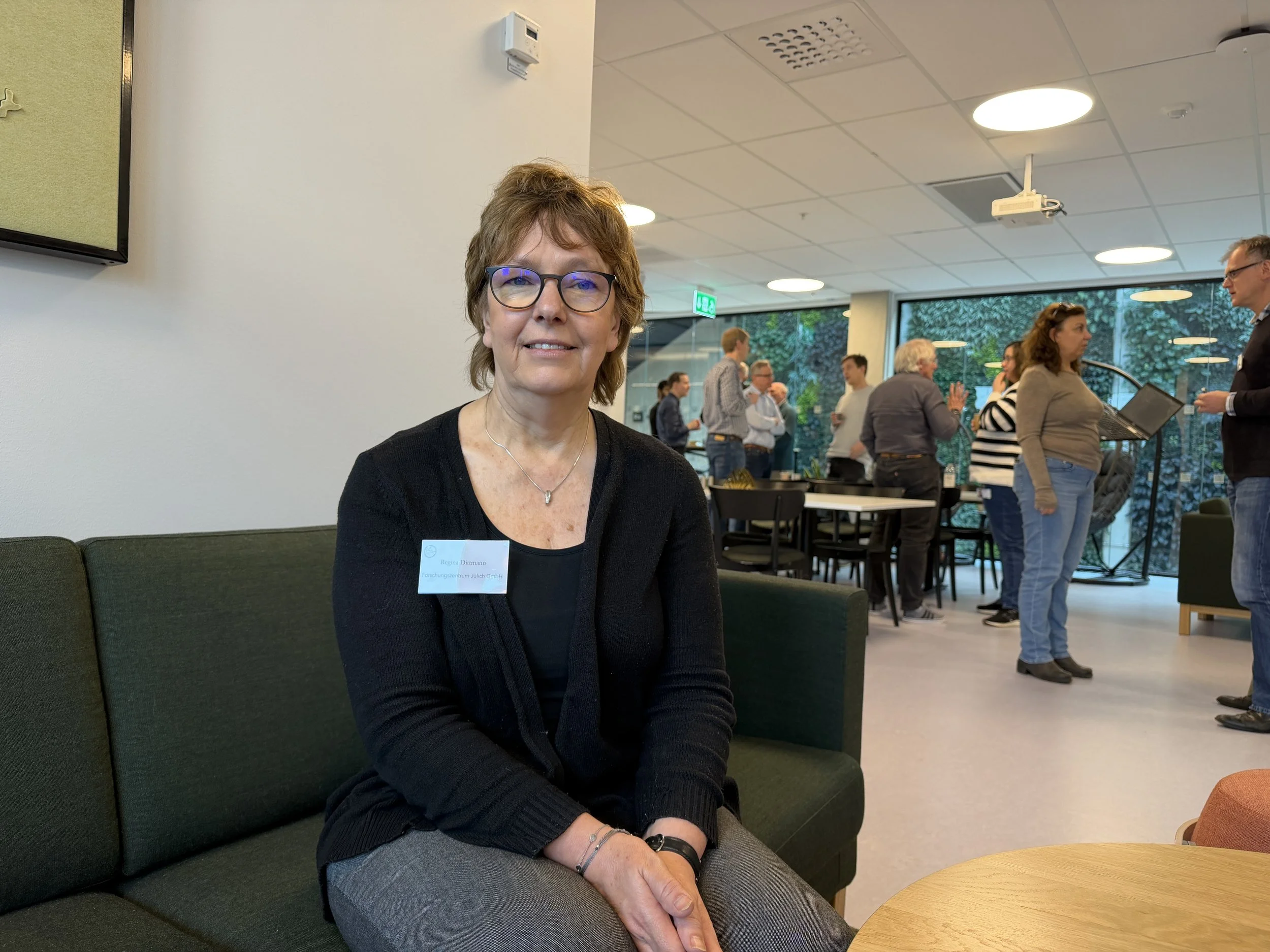
Regina Dittman is looking forward to the work within the theme.
Regina Dittmann, Director at the Forschungszentrum Jülich, GmbH, in Germany, is co-leader for one of the theme’s working groups: Neuromorphic Materials for Deep Learning and AI. Her research is focused on how to use synchrotron techniques to measure microscopic processes in devices – with an aim to develop materials that can serve as vehicles in neuromorphic computing systems. Neuromorphic computing is an engineering approach that mimics neural and synaptic structures in hardware and software to create highly energy-efficient, fast, and intelligent systems.
She is excited about being part of the Semiconductors theme.
“For me, it is very valuable and interesting to have a community to exchange knowledge with. Within the theme, we can engage in new approaches, learn about new techniques, and discuss new aspects of the devices,” says Regina Dittmann.
Bringing researchers and instrument scientists together during the kick-off proved very successful, she says.
“At MAX IV, they are involved in instrument development, something I, and many others, are highly interested in. It was great to hear about what is going on at the forefront of this work, in terms of the development of new techniques and methods.”
Learning across fields and expanding expertise
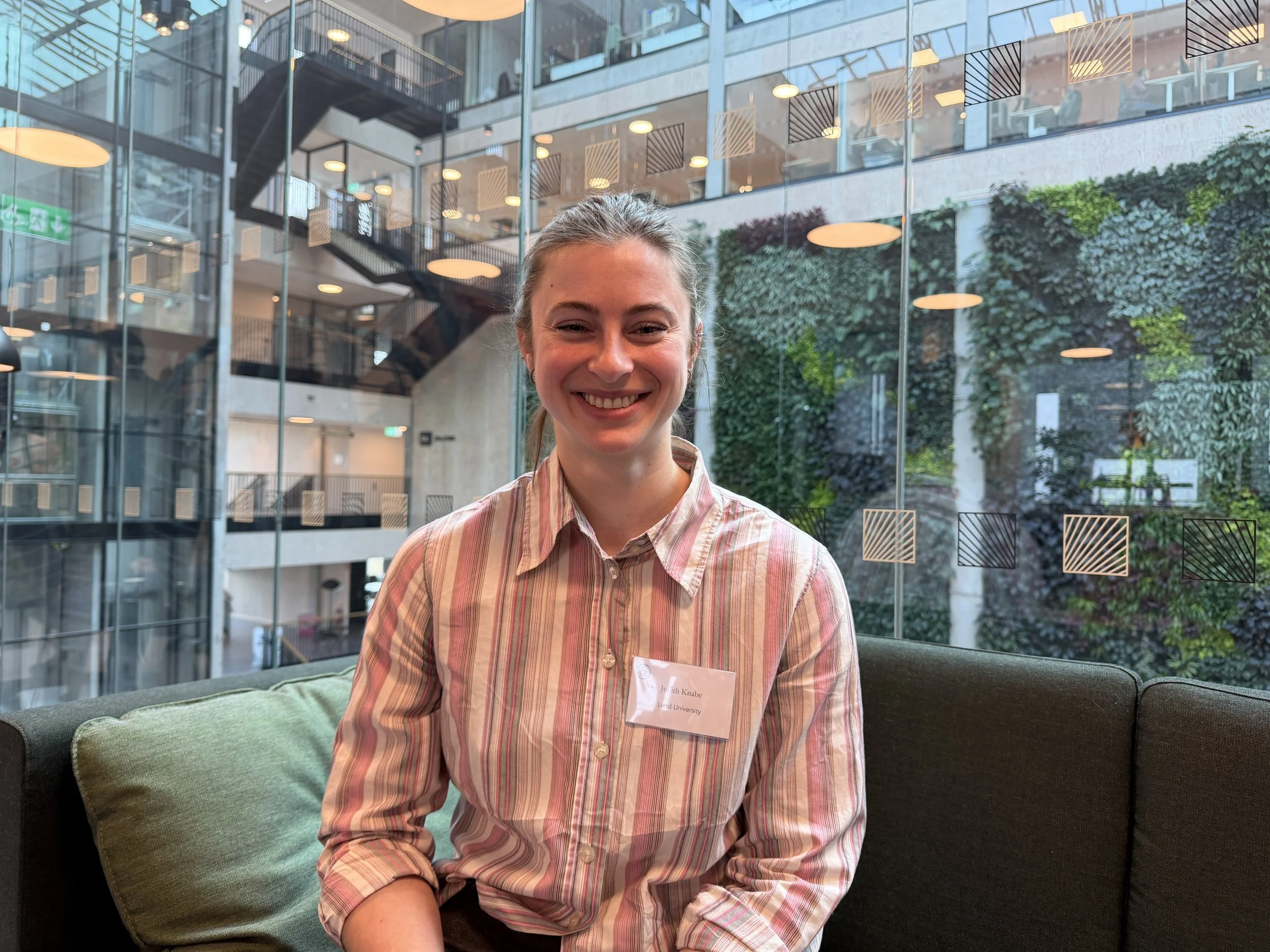
Judith Knabe is excited to learn about new techniques and methods to develop her research.
Judith Knabe is also involved in the theme. She is a postdoctoral researcher in the Department of Electrical and Information Technology at Lund University. In her research, she is interested in developing materials for neuromorphic applications that can be used by industry. From her PhD, which focused on epitaxial films and growth techniques to develop nano-scale electronic and optical devices, she already has experience of X-ray characterisation.
“You are missing out on a lot of opportunities if you are not using these techniques,” says Judith Knabe.
She is excited about learning more about other fields and approaches as part of the theme’s work.
“There is so much more to learn! The theme is a great opportunity to benefit from other people who are experts, and to gain more knowledge of data analysis and different aspects of X-ray and neutron characterisation!”
Kick-off presented new opportunities
Paul Hurley is a Professor at the Tyndall National Institute, at the University College Cork in Ireland. Applying his research expertise in 2D materials and compound semiconductors, he works with developing red microLEDs for next generation of augmented reality (AR)-glasses. Paul and the team are working to characterise, understand and passivate non-radiative defects in the vicinity of the mesa edge of the red microLEDs which are limiting the optical output power. These defects are distributed into the semiconductor (InGaP) over just a few nanometers and remain one of the main challenges for this type of optical AR-technology.
Paul Hurley from Ireland found the kick-off very valuable for his work.
Attending the theme kick-off was an eye opener for Paul Hurley. Learning more about what facilities like MAX IV and ESS can offer was especially valuable.
“I have never been at a synchrotron source before. I found out capabilities I didn’t even know existed!”
“I also learnt about new techniques and approaches we can try in our own research. We have a very specific, but very challenging problem, as the defects on the glasses are only distributed over a few nanometres.”
That the theme brings together different groups of researchers is something he highly commends.
“For collaborations and projects to have a larger impact it is better to gather people that don’t know each other’s work from beforehand. The chance for innovation and breakthrough is much higher. Take me as an example: I am from an electrical engineering background, and I have learnt so many new things from just one visit to LINXS!”